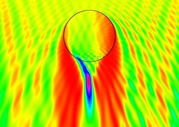
Nanoengineers have invented a spherical nanorobot made of silica that focuses light like a near-field lens to write surface patterns for nanoscale devices. In this image, the red and purple areas indicate where the light is being magnified to produce a trench pattern on light-sensitive material. The researchers published their novel ‘nanomotor lithography’ method recently in the journal Nature Communications. Image credit: Laboratory for Nanobioelectronics, UC San Diego Jacobs School of Engineering.
What does it take to fabricate electronic and medical devices tinier than a fraction of a human hair?
Nanoengineers at the University of California, San Diego recently invented a new method of lithography in which nanoscale robots swim over the surface of light-sensitive material to create complex surface patterns that form the sensors and electronics components on nanoscale devices. Their research, published recently in the journal Nature Communications,offers a simpler and more affordable alternative to the high cost and complexity of current state-of-the-art nanofabrication methods such as electron beam writing.
Led by distinguished nanoengineering professor and chair Joseph Wang, the team developed nanorobots, or nanomotors, that are chemically-powered, self-propelled and magnetically controlled. Their proof-of-concept study demonstrates the first nanorobot swimmers able to manipulate light for nanoscale surface patterning. The new strategy combines controlled movement with unique light-focusing or light-blocking abilities of nanoscale robots.
“All we need is these self-propelled nanorobots and UV light,” said Jinxing Li, a doctoral student at the Jacobs School of Engineering and first author. “They work together like minions, moving and writing and are easily controlled by a simple magnet.”
State-of-art lithography methods such as electron beam writing are used to define extremely precise surface patterns on substrates used in the manufacture of microelectronics and medical devices. These patterns form the functioning sensors and electronic components such as transistors and switches packed on today’s integrated circuits. In the mid-20thcentury the discovery that electronic circuits could be patterned on a small silicon chip, instead of assembling independent components into a much larger “discrete circuit,” revolutionized the electronics industry and set in motion device miniaturization on a scale previously unthinkable.
Today, as scientists invent devices and machines on the nanoscale, there is new interest in developing unconventional nanoscale manufacturing technologies for mass production.
Li was careful to point out that this nanomotor lithography method cannot completely replace the state-of-the-art resolution offered by an e-beam writer, for example. However, the technology provides a framework for autonomous writing of nanopatterns at a fraction of the cost and difficulty of these more complex systems, which is useful for mass production. Wang’s team also demonstrated that several nanorobots can work together to create parallel surface patterns, a task that e-beam writers cannot perform.
The Latest on: Nanofabrication
[google_news title=”” keyword=”nanofabrication” num_posts=”10″ blurb_length=”0″ show_thumb=”left”]
via Google News
The Latest on: Nanofabrication
- Process to set up Kenya’s first semiconductor, microchip fabrication facilities starton April 26, 2024 at 3:50 am
Kenya will host the first semiconductor and microchip fabrication facilities in Africa after Ivhu Africa (Ivhu), an Australian Kenya breaking news | Kenya news today | ...
- Executive Roundtable on The Impact of U.S.-China Relations on Science & A.I. Talenton April 25, 2024 at 12:32 pm
This program is a part of our Seeking Truth Through Facts U.S.-China Program Series, which focuses on new strategic frameworks for the bilateral relationship, plurilateral relationships, rebalancing ...
- Novel Anode Material Boosts Lithium-Ion Battery Performanceon April 25, 2024 at 9:16 am
Dr. Han Joong Tark and student researcher Lee Do Geun at Korea Electrotechnology Research Institute's Nano Hybrid Technology Research Center have devised a novel manufacturing method for ...
- Piezoceramic Plates Market to Reach $3.9 Billion, Globally, by 2032 at 6.8% CAGR: Allied Market Researchon April 25, 2024 at 6:30 am
The piezoceramic plates market is driven by factors such as high piezoelectric activity and high permittivity, and ease of fabricating piezoceramic plates of various sizes, shapes, and requirements.
- Research combines DNA origami and photolithography to move one step closer to molecular computerson April 24, 2024 at 8:49 am
Molecular computer components could represent a new IT revolution and help us create cheaper, faster, smaller, and more powerful computers. Yet researchers struggle to find ways to assemble them more ...
- Making light 'feel' a magnetic field like an electron wouldon April 24, 2024 at 7:29 am
Unlike electrons, particles of light are uncharged, so they do not respond to magnetic fields. Despite this, researchers have now experimentally made light effectively "feel" a magnetic field within a ...
- Mechanical strain control of quantum transport in graphene enables new class of nanoelectronic deviceson April 23, 2024 at 5:00 pm
Integrating strain control with the complex multilayer structures of practical devices will require further innovations in nanofabrication and strain characterization. Nonetheless, by demonstrating ...
- Investors In India Needs Red Carpet, Not Red Tapeon April 22, 2024 at 10:10 pm
India needs many more job creators, both in manufacturing and services, to make it big.' 'For that, the red carpet must be rolled out fully and for all investors without holding back,' suggests ...
- New 2D Polymers Bridge the Gap in Electron Mobility for Organic Semiconductorson April 22, 2024 at 9:09 am
In a recent paper published in Chem, researchers from Pohang University of Science and Technology have developed conducting two-dimensional polymers with electron mobility comparable to graphene, ...
- Researchers discover dual topological phases in an intrinsic monolayer crystalon April 17, 2024 at 10:08 am
An international team working with single-atom thick crystals found TaIrTe4's transition between the two distinct topological states of insulation and conduction. The material exhibited zero ...
via Bing News


